2013-07-13 16:50 UTC
The MC3 CPU board carries 32kB RAM which is actually quite a lot for this kind of computer but more memory is always nice. This memory expansion will increase the available RAM to a whooping 64kB by placing two 16kB pages in the I/O area at $8000-BFFF. This means the we will cover the 128bytes area at $A000 used by MIKBUG. Several applications requires the existence of this memory area to run.
A single 32kB 62256 RAM is used in the design and is divided between two I/O pages, page 6 and 7 (select signals S6 and S7).
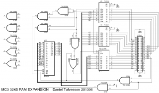
Schematic is seen above. Again no power supply rails are drawn nor are any 100nF capacitors that should be placed over the supply on every chip. All gates are HCT versions despite what the symbol says. Ground the inputs of the unused gates on the left.
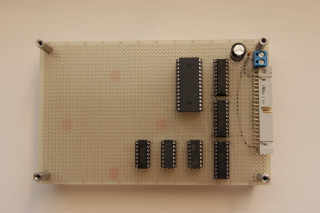
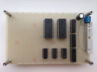
Top of the board. Some room to spare. Perhaps I may squeeze something else in here too. A Compact Flash interface perhaps?
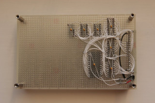
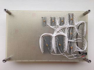
Bottom of the board. Again a soldered board. I found this technique to be quite effective actually. After some practice it is about as fast as good old wire-wrapping. It may be difficult to solder three or more wires on the same point but it can be handled. One thing that is actually better with soldering than wire-wrapping is that you can move a wire from one point to another if you make a mistake. With wire-wrapping you have to scrap the whole wire and do both ends again.
Update 2014-07-30 - Even more RAM!
The urge to make things bigger and better got to me and I added another RAM chip to the current board. There were unused gates on the old board that was sufficient to create the needed address decoding. The only chip that I had to add was the second 62256 chip.
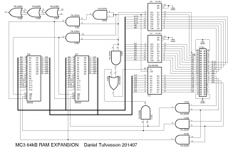
Now the MC3 has a whooping total of
96KB of RAM!
by Nigel 2016-09-10 16:50 UTC
Hi Daniel,
Thanks for all your hard work. I have been building your design and have a working CPU card and compact flash card but was struggling with a non working RAM card.
I now realise why. I think your diagrams have a couple of signals swapped. Pin 6 of IC5 should go to pin 27 of the RAM and pin 8 of IC5 should go to pin 22 of the RAM.
That fixed it for me.
by Daniel 2016-09-22 08:56 UTC
Hi Nigel!
Thank you for spotting this. I have been staring at the schematics now for a while and, yes!, it sure looks like an error on my part. Sorry about that. Hope you didn't waste too much time on it.
I'm really happy so hear that you are building some of my designs and find them useful! Please let me know if there is anything I can do to assist you. And also, please share your work if you can. There are quite a few enthusiasts out there I've realized but few of the designs are put on the web. I have a few more ideas in the making for the MC3 but I have sadly been buried in work this year. Hopefully I'll get some new goodies posted on the site soon.
by sebastian 2020-05-23 03:16 UTC
nice work, even 2020 still interesting to me, while trying to add more RAM to arduino cuz SD card s to slow for my needs..
thanx a lot..
by K8LH 2020-09-15 06:01 UTC
Nice work, Daniel. An elegant solution. Are IC1, IC2, and IC3 buffers & transceiver necessary since those same chips are in place driving CONN1 on the main board?
by K8LH, Michael 2020-09-18 06:52 UTC
Hi again, Daniel. I'd like to build a version using the HD6303YCP (PLCC-68 package) based on Eric Klaus' board design and I'm thinking about using a 64K RAM IC and a 32K 'shadow' ROM. That is, at power-up you read ROM and write RAM in the same address space which allows you to copy the ROM image into RAM, then you toggle one of the port bits to disable ROM and access the 64K RAM. I believe this would allow MIKBUG access to RAM at $A000..$A07F, yes, no? Would you consider looking at my drawing for comments/suggestions/guidance?
Cheerful regards, Mike
by Daniel 2020-09-21 18:42 UTC
Hi Mike! RAM shadowing the ROM sounds like a good plan. I actually did exactly that in one of my earlier 6303 designs. ROM could be swapped out by setting a bit in the 6303 built in I/O port and writes went to RAM regardless of the state of the ROM. That made copying ROM contents to RAM very fast. Just make sure that the ROM is enabled again after reset. That could be done by relying on the I/O port reset state if I remember correctly. The $A000-A007F area is important for many programs as you already discovered. In my opinion a new design should at least have one way to swap RAM into that area for best compatibility. Good luck with your design!
PS. I almost forgot. Yes, I use buffers on all board connecting to the main bus. Depending on the size/length of the bus they may not be needed but it leaves room for expansion and is also a good protection to have on the boards.
Common bus drivers are still in production. Vintage chips are not.
Write a comment