Even though the MC-10 was marketed as a low-end machine, shipping it with only 4k of RAM is extremely limiting even back when it was released. It soon became very clear to me that more RAM was going to be needed in order to do anything useful. There was an official 16k RAM expansion unit that plugged in to the expansion port. I think that was the only official expansion ever released and it was quite common among MC-10 owners. The expansion port of the MC-10 is a little different to, say the Commodore 64, where the expansion port had a dedicated place in the memory address space. In the MC-10 the expansion port has access to every address in the machine and with a single input pin an external device can disable the internal address decoding entirely and place itself anywhere in the address space. Quite flexible actually but it does require relatively complex expansion cartridges. You can not simply create a game/progam cartridge with a single ROM for example.
The expansion port comes with a drawback though. Even if it can insert devices and memory anywhere in the address space, it can not be used to expand the memory accessible by the 6847 VDP since the VDP and internal RAM is hooked up to an internal bus that is isolated from the expansion port.
Since the 6847 VDP can address up to 8k of video memory it would be nice to expand the internal 4k RAM on that internal bus to 8k so that the full potential of the 6847 could be utilized. There was actually an article published in 1987 that explained such a modification. It involved piggybacking two more 2k SRAM chips on top of the existing ones and add some additional decoding. Today I would not recommend following that article. Not only does the article contain a few critical errors but it's just an unnecessarily complicated mod that adds four more chips, and piggybacking the RAM chips makes the RF shield not fit any more. I have another approach that involves just swapping the two onboard 2k RAM chips with a single 8k RAM chip. Actually the end result is reducing the total chip count by one.
Theory
The MC-10 address decoding is a bit odd but relatively simple. The address space is divided into four 16k areas, each with it's own select lines for read, and write where applicable. These select lines are generated from address lines A14 ad A15 by U4 74LS155. The second set of select lines ($4000-$7FFF) are used for the two internal RAM chips. Since they are smaller than the 16k area they are assigned, the memory will show up repeated four times within this area. This confuses MS BASIC so that it detects all 16k as available memory. In order to fix this RadioShack bodged on an extra 74LS32 that gates the write signal to the RAM with address line A12 which effectively block writes to the first and last mirror of the 4k RAM in the 16k area. This makes MS BASIC happy and correctly detects the first 4k as available memory.
To make the 6847 VDP able to access all the 8k of new RAM we have to make use of its unconnected DA12 pin. The original design uses two buffers to isolate the CPU A0-A11 from the VDP DA0-DA11 address lines. The two 74LS367 buffers have no available gates to accommodate A12/DA12 and I did not want to add another big chip just for that so took a shortcut. The same way I did when designing my MC3 video card, I used a single resistor to multiplex the two address lines together. This works since the access to RAM is multiplexed, the CPU and VDP never tries to access the RAM at the same time, and the VDP is nice and tri-states the DA0-DA12 lines when not accessing the bus. Hooking the VDP DA12 pin up to the RAM directly and the CPU A12 pin via a resistor makes up a crude multiplexer where the VDP always "wins" when it has access to the bus and backs off (tri-states) when the "weak" CPU has access to the bus.
Putting it all together
My idea is to remove the two internal 2k 4016 RAM chips and replace them with a single 8k 6264 RAM chip. Luck have it that the bigger 6264 is in large part pin compatible with the smaller 4016, even though the 4016 is a DIP24 and the 6264 is a DIP28. Only a few pins need to be bent out and re-arranged to make this work.
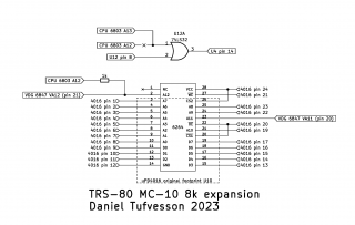
This is the schematic of the modification. The 6264 will be soldered in place of one of the two 4016 chips (I used U10) . The legs 1, 2, 20, 23, 26, 27, and 28 of the 6264 bent out to the side, parallel to the board and away from the 4016 footprint. With the legs bent out the 6264 will fit into the board instead of the 4016. Then it's a matter of running a few wires around to hook up the remaining pins. Use the schematic and photos below for reference. Note that pin 1 of the 6264 is not used and should be left unconnected.
The top 74LS32 gate in the schematic illustrates the bodge wire from U12 that needs to be moved from address line A12 to A13. The signals are easiest to reach using the vias as in the picture. There is no need to cut the existing A12 wire, just move it to the other via, so this mod is 100% reversible.
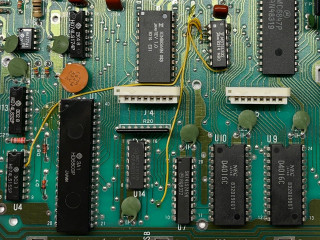
For reference this is what the board looks like before the modification. The two 4016 RAM chips down to the right. Both will have to be removed. As always some care must be taken while desoldering and don't rush it. (As usual if you are not confident removing components like these please please please stop here.)
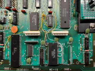
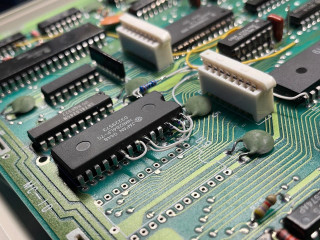
This is the completed modification. The 6264 soldered onto the board without socket. This is a personal preference. It's not possible to use a socket and still be able reattach the RF shield.
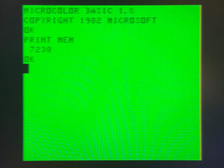
With this modification MS BASIC now has 7238 Bytes free and the VDP can access the whole 8k address space!