After completing and testing the QSD/QSE module and the BPF module, I knew the basic concept of the transceiver was living up to my expectations (see
part 4 and
part 5 for more information) and now I had to take a step back to figure out how to bring this all together into a self contained radio.
My main mode of operation is SSB and I think I share that with many others. Having SSB makes it possible to also receive AM and CW which probably covers most, if not all, of my needs. CW TX is trivial to add later since it's just a carrier.
The QSD/QSE module works with I/Q signals on the AF/LF side and while I/Q signals can represent more ore less any traffic mode (AM, FM, SSB etc) it requires quite a lot of processing to be useful. In order to make this transceiver operate on SSB I need to phase shift the I and Q signals precisely 90 degrees from each other over the entire modulation range, say 300Hz-3000Hz. Nowadays this is normally done in software but I really want to try doing this the analog way using all-pass phase shift networks and see if I can make it good enough for general use.
Basic concept
Below is a block diagram of the basic layout of the transceiver that I have in mind (click to enlarge). This is most likely going to change as the project progresses but for now it sums up the general idea and concept.
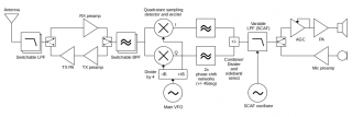
The two parts that are completed are the switchable BPF module and quadrature sampling detector/exciter module. In this write-up I will cover components to the right of the QSD/QSE, starting with the phase shift networks for processing the I/Q signals and convert them to and from AF signals.
My idea is to create two all-pass filter networks, one for the I path and one for the Q path, and have them shift the phase +45 degrees and -45 degrees respectively. That way the total shift between I and Q will be 90 degrees. The naive approach would be to use only one 90 degree phase shift network on either the I path och the Q path, but doing it this way will limit the phase shift done in each network, making them perform better. I also want the filters to have the ability to change direction so that the same filters can be used for both RX and TX. There is a lot of fine tuning involved in these filters and doing it this way, besides reducing the number adjustment points by half, also ensures that the transmit performance will be about as good as the receive performance. It's a good sanity check.
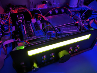
Mechanical construction
For the AF/LF parts of the transceiver I decided not to use individually shielded boxes, as I did it for the RF modules since it adds considerable amount of metal work compared to the performance gain (this may come back and bite me in the end). I decided to stack two half eurocards (100x80mm) with standoffs. Bottom board for the digital parts and top board for the analogue parts. These are interconnected by a 20pin ribbon cable. By separating this into two boards I hope to reduce the self-induced digital noise. The phase shift board/module is mounted on top of the analogue board.
All-pass filter phase shift module
This is the core of what makes this a self contained SSB radio. The idea here is to have a module that inputs I/Q signals on one side and outputs single sideband audio on the other side, as well as the reverse to make it work for both RX and TX. It should also have the ability to select upper or lower sideband. Below is the module I came up with.
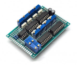
By just looking at the number of trimmers on this board one can expect quite a bit of tweaking but it's mostly due to the fact that the all-pass filter requires very specific resistor values. The design is based around two four pole all-pass filters with an optimized frequency range of
200Hz to 4000Hz. That should cover normal SSB traffic with some margin. The filter will only suppress the sideband for frequencies that are inside of this range. This means that the filter must be used together with corresponding band-pass filtration. Below is the schematic for the phase module.
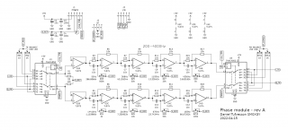
The all-pass filters are made up of two quad TL074 op-amps (U3 and U4). The resistors, trimmers and capacitors here must be high precision and low tempco. The trimmers set the frequency for each pole. In the schematic I have included the calculated pole frequencies and corresponding trimmer values. I used my Keithley 196 multimeter with kelvin clipleads to measure and adjust the trimmers in circuit after soldering to be as close as possible to the calculated values.
Before the filters is a dual TL072 op-amp amplifier, U2, acting as a buffer to ensure high input impedance and constant drive to the filter.
To do all the switching between TX and RX as well as selecting USB or LSB, I used two 74HC4052 dual channel four way analog switches. One on the input to the filter, U1, and one on the output of the filter, U5. I was very happy when I realized I could use these switches. It made the design very clean.
During receive the signal flow is:
I_RX & Q_RX --> AF_DEMOD
and during transmit the signal flow is:
AF_MOD --> I_TX & Q_TX
During receive the output of the filters are summed into a trimmer, one trimmer for LSB and one trimmer for USB. The same arrangement goes for the input to the filter during transmit. That way the signal balance can be individually adjusted for all the four situations, LSB RX, USB RX, LSB TX and USB TX using the trimmers RV1, RV2, RV11, RV12.
For selecting LSB or USB the filters are swapped between the I path and the Q path.
One bonus feature of the 74HC4052 is that there is an enable input. Pulling this input high disables all switches and puts the module into a high impedance state. That makes it possible to connect multiple modules like these in parallel and select between them in software by setting this logic pin. The mechanical design I use makes it possible to stack multiple boards using pin headers. I have not yet tried this but it's an interesting expansion possibility. Dedicated narrow CW module maybe? AM? FM? We'll see...
Update 2023-01-06
Can't believe I forgot to mention where the filter values are derived from. I spent quite some time reading and trying out various algorithms but in the end component quality and overall construction had a far greater impact on my end result than finding the absolute optimum algorithm. The
J-TEK all pass filter designer software by GJ3RAX is a very good start. Great piece of software. In my opinion experimentation is needed to find the optimal values. The resistor values in the schematic will get you in the ball park. To get full performance out of the filter each pole must be adjusted individually. To do this, hook it up on the bench and jumper it to TX mode and any sideband. Then use a signal generator to input each frequency in turn and adjust each pole for 90 degree phase shift by measuring each pole input and output using a two channel scope. Either use the scopes built-in phase meter or set it to XY mode and adjust for best looking circle.
Main analog board
This board is still very much under development but I figured I would post parts of it since it contains the very important band pass filter required by the phase module described above. The phase module sits as a mezzanine board on top of the main analog board and connects using three sets of pin header. Since the phase module only works for a specific audio band, the audio going in and out of the module must be filtered. This filtering is done on the main board. Below is an excerpt from the analog board showing the RX/TX audio switching and audio band pass filter.
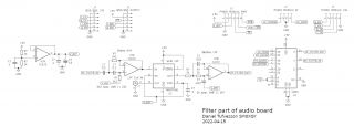
I based the filter around the well known MAX7400 switched capacitor low pass filter to make the bandwidth adjustable from software. It's currently driven by a spare output of the Si5351 signal generator. The drive frequency is 100 times the crossover point. The MAX7400 is then combined with a 300Hz high-pass filter on the input and a 3600Hz low-pass filter on the output. The low-pass filter is important since the MAX7400 will leak the drive frequency to the output, but being 100 times above the crossover frequency it's easy to filter out.
To be able to share the filter between both RX and TX, I added a HC4053 analog switch.
Outside of the schematic the RX_AUDIO signal goes to an AGC controller and the final audio amplifier, and the TX_AUDIO comes from the microphone amplifier and dynamic processor. There are also logic level control signals in the schematic but I think they are quite self explanatory. They are all coming from a separate CPU/logic board that I will present later.
Performance
I have not yet performed any proper measurements regarding sideband suppression but after many evenings on the bands I can tell that it works surprisingly good. Definitely better than my Icom IC-735 reference transceiver. Using earphones and swapping sideband on an ear-shattering signal completely wipes it out and pushes it down in the noise. Good enough for me.