The world is in a weird state right now. I hope you are all doing well. For me this stay-at-home and work-from-home situation has at least given me some time to re-evaluate my shortwave transceiver project. To be honest I wasn't happy with the performance I got out of my superheterodyne design. It got more and more complex in order to achieve good performance across the intended shortwave range. It got complex to the point where I deviated far away from the goal of making a simple, understandable and yet decent performing transceiver out of common off-the-shelf parts. Either way I turned and twisted my design it ended up being too much of a compromise for my liking. This was not what I had in mind at all. Let's just say there is a reason good performing transceivers of this kind are expensive. Dealing with multi stage mixing and filtering is powerful but doing it right takes a lot of careful calculations and filtering. Also every stage of the transceiver also impose a risk of degrading the signal (i.e. by introducing noise and intermodulation) making each stage even more complex and critical. To reach my goal I had to find another way.
Direct conversion
The surprisingly good performance from my
earlier experiment with the NE612 direct conversion receiver got me thinking.
What if an advanced direct conversion design is actually less complex than a relatively simple superheterodyne design?
Two common problems with direct conversion is carrier leakage and the ability to distinguish between upper and lower side band (since it's only a single conversion stage). Carrier leakage is a potential problem because the mixer is running at the operating frequency which can cause various issues as well as undesired radiation of a carrier signal even in receive mode. This can be mitigated by good RF isolation, careful mixer design and a receive pre-amplifier. Then there is the question about demodulation and modulation. A single mixer stage, as used in most simple direct conversion designs, will effectively act as a DSB receiver/transmitter with no way of distinguishing between upper and lower side band so we need something better. An answer to this is quadrature signals. This is achieved by using two mixers connected to the same RF-input. These two mixers are fed from a local oscillator that generates two signals with a very exact 90 degree phase offset, one for each mixer. This results in two mixing outputs. One in-phase signal,
I, and one signal,
Q, that is phase shifted 90 degrees.
Having the I and Q signals and knowing the phase relationship between the two it's possible to determine the location of any given signal within the pass-band. Signals with exactly 90 degrees phase offset between I and Q belongs to one of the sidebands (+90 for one sideband and -90 for the other). This again is bidirectional and works for both demodulation and modulation.
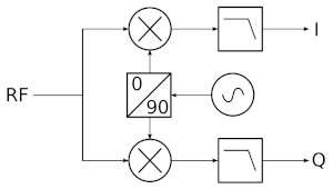
Diagram above shows a typical quadrature mixer which can be realized with a pair of double balanced mixers such as the SBL-1. This kind of mixers however are not ideal for this use-case. They are very sensitive to input and output termination which makes them complicated to use in a wideband scenario and the conversion loss is also relatively high. One very nice thing though is that the design can be made to be bidirectional making it possible to use the same mixer for both receive and transmit. The quadrature concept requires symmetry. Both mixers must be equal. Good off-the-shelf balanced mixers are also relatively expensive and the manufacturing tolerances are usually not good enough and will require matching of two mixers for good result. Lately there is a new way to do this that has become very common and that solves most of these issues.
Quadrature sampling
This principle is used in many software defined radios today. A good performing quadrature detector can be built using a modern digital multiplexer. After some initial testing I decided to give this a try.
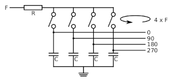
The principle is quite simple. There are four switches and four sampling capacitors. The detector cycles through all four switches in turn at a frequency that is four times the desired mixing frequency. That means that each switch is activated one time for every cycle which creates a 90 degree phase offset between each switch (360/4=90) and since there are four switches the frequency for which each switch is activated will be the desired switching frequency. The fact that there are now four outputs is very useful since the 0 and 180 outputs can be treated as a balanced
I signal, and the 90 and 270 outputs can be treated as a balanced
Q signal. The design can act both as a
detector by feeding an RF signal into it and amplifying the balanced I and Q signals, or as an
exciter of an RF signal by feeding it with balanced I and Q signals.
Together, the system impedance, R, and the sampling capacitors, C, makes up a low pass filter. This determines the bandwidth of the detector and also causes the input impedance to peak at the center frequency and drop off towards either side. To some extent the "Q" factor of the filter will also vary with frequency.
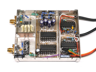
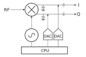
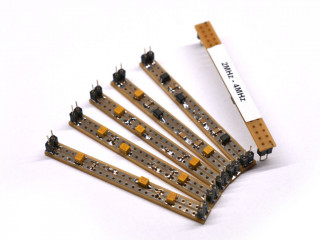
My combined QSD/QSE module
I wanted build a module that incorporated both a
Quadrature Sampling Detector and a
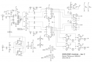
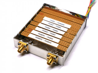
Quadrature Sampling Exciter into the same unit sharing the same RF input/output port and cover 0-30MHz. That way I could simply swap this module into my existing transceiver design replacing the first mixer, crystal filter, product detector, modulator, as well several amplifier stages. Actually just combining this module with a suitable band pass filter would make up a complete RF section of a low power transceiver. The QSD in itself is sensitive enough to perform well even without a preamplifier. Since the I and Q signals are balanced the common mode rejection is very good making it is possible to follow the detector by high-gain amplifiers. Below is a picture of the module that I came up with.
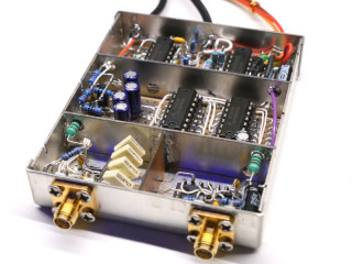
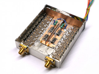
As mentioned earlier and after some experimentation it became obvious that there was a lot to gain from RF isolation so I decided to build this module into a metal enclosure. I also sectioned off the inside of the module to further improve isolation. There are SMA connectors for RF input/output and local oscillator input. The TX/RX I/Q signals are fed through shielded microphone cables.
Design details
The module is divided into four compartments.
-
Top left: FST3253 switch and sampling capacitors
-
Bottom left: 74AC74 quadrature clock generator
-
Middle: 74HC4053 multiplexers for TX/RX switcing
-
Right: TL074 TX/RX I/Q amplifiers
 Update 2021-06-15 rev C
: Moved Q_BAL to positive side of Q (90 deg instead of 270 deg). Does not affect performance but this way the calibration values makes more sense. Replaced TL074 opamps with the better performing NE5234. R26-R29 no longer needed. Fixed U5E flipped supply in schematic (thanks oz9ny!). See
rev B.
Update 2021-02-16 rev B: Moved R26-R29 so that they are shared for both TX and RX. See
rev A.
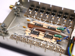
The schematic is laid out similar to the real layout. The front end of the module and mixer consists of the FST3253 switch. It is a common device to use for this purpose and is known to perform well. It is fast and has relatively low on-resistance. One minor downside is that it does not come in a DIP so in this case I use the SOIC version. It did not matter very much since this compartment is built in dead-bug style anyway to help with symmetry and RF performance. The four sampling capacitors (C5-C8) are soldered directly to the legs of the FST3253. I matched four out of a batch of 50 that came within 1% of each other. The quality of these capacitors are important. I used R82 polyester capacitors for this. The two switch banks of the FST3253 are connected in parallel to further decrease on-resistance and the input is biased (R4,R5) at Vcc/2=2.5V. Also there is a resistor, R3, in series with the RF input/output. Depending on the rest of the design this resistor may or may not be needed (keep in mind that resistance here increase noise and reduce gain) but it can be used to maintain 50 Ohm impedance. Preferably it should be left out but may be needed to play nice with other components. I measured the output impedance of my module and it ended up being closer to 35 Ohms so I set R3 to 15 Ohms. The FST3253 is driven by a quadrature clock that can be treated as grey-code to activate the switches one at a time in sequence.
The quadrature clock is derived from an external local oscillator at four times the desired mixing frequency. One fast dual flip-flop 74AC74 is used to convert the incoming clock into two clocks at a quarter of the frequency but 90 degrees apart. To reach a 30MHz mixing frequency the external oscillator must be able to operate up to 30x4=120MHz. This means the faster 74AC74 must be used. Slower versions such as the 74HC74 or 74HCT74 will not work. Because of the high frequency this part is also built using dead-bug style. In-line with the quadrature outputs are 100 Ohm resistors (R6,R7). These resistors rounds off the signals slightly and reduces over tones. The resistors are actually placed right in the middle between the compartments to also act as feed-trough devices. The power supply to the 74AC74 is extra filtered (+5VD). Not because of any extreme demands from the 74AC74 but to prevent switching products to exit and reach other parts of the module.
The middle compartment consists of the four "big" bipolar DC blocking capacitors (C15-C18) as well as the two 4053 multiplexers used for TX/RX switching. It also contains parts of the active balancing circuit but more on that later. The two 4053 switches the balanced I/Q signals from the FST3253 between the TX/RX I/Q amplifiers in the rightmost compartment. These amplifiers are based on TL074 operational amplifiers. There are better alternatives but I had these at hand and they performed reasonably well as a start. The most important thing is to maintain symmetry between the I and Q paths, therefore all of the resistors here have 1% tolerance or better. I actually used 0.1% precision resistors instead since that's what I had at hand.
Update 2021-06-15: In revision C of the design I replaced the TL074 amplifiers with the better performing NE5234. They are drop-in replacements and provides better linearity, better sensitivity, higher output along with reduced distortion.
About 10 times more expensive but definitely worth it.
Initial results
To test the module I used two signal generators and observed the mixing products on a scope.
Example test setup:
- LO = 28.000MHz 0dBm (Fluke 6060A)
- RF = 7.001MHz -40bBm (HP 3325A)
- I/Q signals hooked up to scope (Tektronix TDS2014C) in XY mode
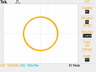
As you see here a 90 degree phase difference between the, in this case, 1kHz I and Q outputs generates a circle on the scope. This is what we want. The module was working!
But it soon became apparent that more work was needed. Performance was inconsistent over the 0-30MHz operating range. The symmetry varied and in some parts, mainly over 25MHz, the dynamic range was noticeably limited. Also the carrier suppression was not good enough for my liking and varied a lot over the entire range (best 40dBc and worst 20dBc). This got me puzzled for quite some time until I started poking around with a high impedance high resolution volt meter directly at the sampling capacitors. What I found was that the DC levels varied with the local oscillator frequency and was never really equal and often far from the expected 2.5V they were biased at from the "front" side of the mixer. Now things started to make more sense. The question was what caused it and how to solve it.
Active balancing
Disconnecting the DC blocking capacitors (C15-C18) thus isolating the detector from the rest of the circuit did not improve the situation. Even more careful matching of the sampling capacitors did however improve the balance problem a bit but not to the point that it was good enough. I was going to need something more than just well matched components.
That's when I discovered that it was possible to bias the mixer from both sides by loosely injecting a DC voltage onto the I and Q signals, directly at the sampling capacitors. The bias compensation needed was still very frequency dependent but solved all of the problems, when adjusted properly. I added two filtered DC inputs to the module, I_BAL and Q_BAL, that connects directly to two of the sampling capacitors, one on the I side and one on the Q side. First I was afraid I would need four bias signals but it turned out that the over all I/Q balance is what matters so the DC offset can be injected to either one of the I and Q capacitors.
Since the needed bias compensation varied with frequency I figured I could solve this in software by adding two DAC outputs to my Si5351 based local oscillator controller. I used a pair of PCF8591 8-bit DACs and by experimentally selecting values for R8-R11 it was possible to utilize the full range of the DACs which turned out to be more than enough resolution. These resistors along with the capacitors between them makes up a very important low-pass filter since these signals are injected directly into the signal path. I use a lookup table along with linear interpolation in software to generate the DAC values. Finding the correct values for I_BAL and Q_BAL is a matter of nulling out the carrier. As a start I adjusted these values for every even MHz within the operating range and interpolated between them. It turned out to work very well! Now the module performs very good from 0-30MHz with a carrier suppression of around 50dBc to 60dBc.
Conclusion
This has been a fun part of my transceiver project. Finally I feel that I have completed a central part of what I need to build the reasonable performing rig I initially set out to make. Initial testing by connecting the I/Q signals to a PC with SDR software worked surprisingly well and with very good band suppression. The next step is to construct a switchable band-pass filter module to go before the QSD/QSE module. Then there is the question of analog phase shifting networks for a fully analog approach but further experimentation will tell which way I will go.
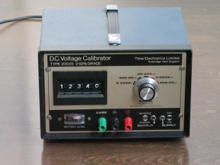 I've had this Time Electronics 2003S Voltage Calibrator on the shelf for a very long time. It never worked. The output was way off and with several mV of ripple and oscillations at around 400-700 Hz. From time to time I've been working on it but never really got anywhere. The reason is that the core part of this instrument is rudely enough potted in epoxy. After going through everything within reach I realized the the problem was inside that nasty slab of hardened goop.
I will spare you the details of the massacre that followed but after hacking away at this using acetone, heat and chisel, I eventually gained a peak inside the module only to sadly discover the, somewhat expected, state of bulging and fishy smelling leaking electrolytic capacitors and corrosion. I had spent hours already and was not going to spend all the time needed to refurbish this nasty design that was clearly intended to prevent repairability in the first place. I threw the module in the bin.
This however left me with a nice base to rebuild the instrument. Let's have a closer look.
The front panel comes off easily and contains all major parts of the device except for the power supply that is mounted in the back of the box. The device can be battery powered but I removed the batteries and disabled the trickle charger circuit a long time ago to prevent damage from leaking batteries. Now it's just a basic 18V linear power supply regulated by the somewhat uncommon 7818 voltage regulator. Not very interesting. Let's focus on the front instead.
I've had this Time Electronics 2003S Voltage Calibrator on the shelf for a very long time. It never worked. The output was way off and with several mV of ripple and oscillations at around 400-700 Hz. From time to time I've been working on it but never really got anywhere. The reason is that the core part of this instrument is rudely enough potted in epoxy. After going through everything within reach I realized the the problem was inside that nasty slab of hardened goop.
I will spare you the details of the massacre that followed but after hacking away at this using acetone, heat and chisel, I eventually gained a peak inside the module only to sadly discover the, somewhat expected, state of bulging and fishy smelling leaking electrolytic capacitors and corrosion. I had spent hours already and was not going to spend all the time needed to refurbish this nasty design that was clearly intended to prevent repairability in the first place. I threw the module in the bin.
This however left me with a nice base to rebuild the instrument. Let's have a closer look.
The front panel comes off easily and contains all major parts of the device except for the power supply that is mounted in the back of the box. The device can be battery powered but I removed the batteries and disabled the trickle charger circuit a long time ago to prevent damage from leaking batteries. Now it's just a basic 18V linear power supply regulated by the somewhat uncommon 7818 voltage regulator. Not very interesting. Let's focus on the front instead.
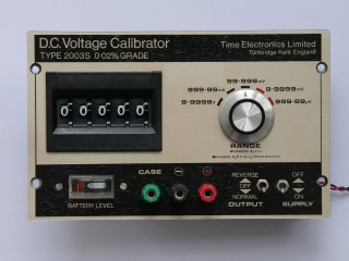 The front panel is quite self explanatory. There are five ranges selected by the knob to the right and the desired output voltage is entered with five digits resolution using the switch on the left. The difference between each range is a factor of ten.
Range 1: 0-9.9999 V
Range 2: 0-999.99 mV
Range 3: 0-99.999 mV
Range 4: 0-9.9999 mV
Range 5: 0-999.99 uV
No surprises so far. The front panel contains all the things you would expect. However flipping the panel over reveals a pretty nice PCB with guard rings and populated with precision resistors and trimmers. The connector on the left is where the epoxy potted module would connect.
The front panel is quite self explanatory. There are five ranges selected by the knob to the right and the desired output voltage is entered with five digits resolution using the switch on the left. The difference between each range is a factor of ten.
Range 1: 0-9.9999 V
Range 2: 0-999.99 mV
Range 3: 0-99.999 mV
Range 4: 0-9.9999 mV
Range 5: 0-999.99 uV
No surprises so far. The front panel contains all the things you would expect. However flipping the panel over reveals a pretty nice PCB with guard rings and populated with precision resistors and trimmers. The connector on the left is where the epoxy potted module would connect.
 The manual and schematics are available online. Or rather part of the schematics. Unfortunately the schematic for the potted module is not in those files. It is only mentioned that in case of problem with the module it could be sent in for replacement. Probably not going to happen for an over forty year old instrument. However the manual also states that the module contains the voltage reference and a chopper stabilized amplifier. This is very useful information.
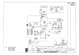 Above is the schematic from the available documentation (I erased the parts for the 2003N that is not applicable here). It matches the board inside the meter. The component marked "2003 circuit module" is the epoxy potted module. That is just a black box but doing the math backwards using the resistors on the board reveals that the module is simply an inverting op-amp. An inverting amplifier also means that voltage reference is negative. About -6.294V.
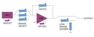 This is the block diagram of the 2003S. It's a voltage reference and an amplifier with variable gain plus an additional attenuator for the low ranges. The active components marked REF and AMP are what's inside the module and the resistors and switches are on the PCB. This is really good. It means that all of the critical components for voltage selection are on the PCB and not in the module!
Armed with this new knowledge I set out to design a proof of concept replacement module.
This is the block diagram of the 2003S. It's a voltage reference and an amplifier with variable gain plus an additional attenuator for the low ranges. The active components marked REF and AMP are what's inside the module and the resistors and switches are on the PCB. This is really good. It means that all of the critical components for voltage selection are on the PCB and not in the module!
Armed with this new knowledge I set out to design a proof of concept replacement module.
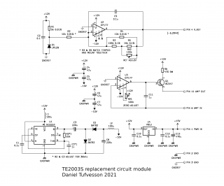 On the top of the schematic is the voltage reference. High performing voltage references are a whole other topic. This is a naive design around an LM129 reference zener and an OP177 op-amp. Good enough for a start but time will tell if it will be enough to meet the original specifications of the instrument. The LM129 provides a 6.9V reference and the OP177 is wired up as an inverting amplifier. The resistors R2 and R4 are equal and matched, which sets the gain of the OP177 to unity and inverted (-1). This is actually too much since we need a lower gain of around -0.912 to achieve the desired reference voltage of -6.294V. To nudge the amplifier gain down a bit, R4 is paralleled with a set of fixed resistors and a trimmer. The specs of these resistors are not as good as R2 and R4 but their values are selected to affect the gain just enough to reach the desired level. Therefore their impact on the final performance is reduced.
In the middle is the main amplifier responsible for the actual output of the instrument. This amplifier have its feedback and gain setting resistors on the main PCB and knobs and dials. Even though the original design used a chopper amplifier I opted to try using the OP177 here as well. I did however buffer the output a little extra using a BC547 transistor and an oversized series power resistor to handle eventual shorted output terminals. The output driver transistor is also fed directory from the main supply to keep load off the local 12V supply.
At the bottom is the power supply. Not much to say here. A positive 7812 regulator provides local 12V and a DC/DC converter based on a 555 provides -10V. The 12V rail stability is most important here since it also powers the LM129 reference.
Note that there are two different grounds. One for the supply and one for the reference. Both end up in the same ground point on the main PCB to provide a star ground.
On the top of the schematic is the voltage reference. High performing voltage references are a whole other topic. This is a naive design around an LM129 reference zener and an OP177 op-amp. Good enough for a start but time will tell if it will be enough to meet the original specifications of the instrument. The LM129 provides a 6.9V reference and the OP177 is wired up as an inverting amplifier. The resistors R2 and R4 are equal and matched, which sets the gain of the OP177 to unity and inverted (-1). This is actually too much since we need a lower gain of around -0.912 to achieve the desired reference voltage of -6.294V. To nudge the amplifier gain down a bit, R4 is paralleled with a set of fixed resistors and a trimmer. The specs of these resistors are not as good as R2 and R4 but their values are selected to affect the gain just enough to reach the desired level. Therefore their impact on the final performance is reduced.
In the middle is the main amplifier responsible for the actual output of the instrument. This amplifier have its feedback and gain setting resistors on the main PCB and knobs and dials. Even though the original design used a chopper amplifier I opted to try using the OP177 here as well. I did however buffer the output a little extra using a BC547 transistor and an oversized series power resistor to handle eventual shorted output terminals. The output driver transistor is also fed directory from the main supply to keep load off the local 12V supply.
At the bottom is the power supply. Not much to say here. A positive 7812 regulator provides local 12V and a DC/DC converter based on a 555 provides -10V. The 12V rail stability is most important here since it also powers the LM129 reference.
Note that there are two different grounds. One for the supply and one for the reference. Both end up in the same ground point on the main PCB to provide a star ground.
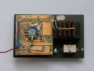
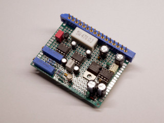 This is the complete replacement board. I salvaged the connector from the potted module (only a small part of a corner was lost in the process). One important thing to mention here is the choice of components. As you see there are no crazy high end resistors. I simply did not have suitable alternatives at hand and component shortage is no joke at the moment, so I did the best I could with what I had. I will need to improve that once I manage to source proper ones. I probably also should get rid of the IC sockets to lower the thermal EMF.
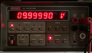
One thing I did however was to match the temperature coefficient on the U2 gain setting resistors R2 and R4. These resistors set the base gain of the reference amplifier as described above and need to be equal. The theory here is that the values of R2 and R4 will vary with temperature and it is okay for R2 and R4 to vary a small amount as long as the amount of change is the same in both resistors. This is where their temperature coefficients comes in. The way I did this was to heat up a container of mineral oil to around 50C and then use a 6.5 digit multimeter (my Keithley 196) with four point kelvin leads to measure a batch of 25ppm/C resistors until I found two resistors that exhibited the same resistance change when dipped into the oil. Then I mounted these two resistors close together on the board.
This is the complete replacement board. I salvaged the connector from the potted module (only a small part of a corner was lost in the process). One important thing to mention here is the choice of components. As you see there are no crazy high end resistors. I simply did not have suitable alternatives at hand and component shortage is no joke at the moment, so I did the best I could with what I had. I will need to improve that once I manage to source proper ones. I probably also should get rid of the IC sockets to lower the thermal EMF.
One thing I did however was to match the temperature coefficient on the U2 gain setting resistors R2 and R4. These resistors set the base gain of the reference amplifier as described above and need to be equal. The theory here is that the values of R2 and R4 will vary with temperature and it is okay for R2 and R4 to vary a small amount as long as the amount of change is the same in both resistors. This is where their temperature coefficients comes in. The way I did this was to heat up a container of mineral oil to around 50C and then use a 6.5 digit multimeter (my Keithley 196) with four point kelvin leads to measure a batch of 25ppm/C resistors until I found two resistors that exhibited the same resistance change when dipped into the oil. Then I mounted these two resistors close together on the board.
 Now the 2003S is back to life. Or at least now I can start using it and determine the actual performance over time. It takes quite a while for the components to settle. For now I will just keep it running for a few months and monitor the performance. A rough estimate is that it currently settles within it's relatively relaxed "0.02% grade" as long as the ambient temperature is kept under control. The temperature coefficient need improvement but at least the design is relatively sound. Resistors with higher precision and better stability will improve stability significantly once I manage to source some.
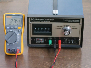 At least in its current state the 2003S is good enough to verify something like a 3.5 digit multimeter. This was a fun little project. My main take-away from this is that metorology is complex and your measurements are only as good as your trust in your reference. And an old instrument with known good and recorded calibration history may be more worth than that fancy expensive shiny new one right out of the factory.
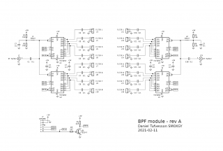

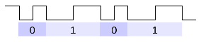 One cycle of a high frequency represents "0" and a single cycle of low frequency represents "1". This effectively makes ones and zeros have different length. That means the average bit rate will vary depending on the distribution of ones and zeros.
2. Varying pulse lengths
One cycle of a high frequency represents "0" and a single cycle of low frequency represents "1". This effectively makes ones and zeros have different length. That means the average bit rate will vary depending on the distribution of ones and zeros.
2. Varying pulse lengths
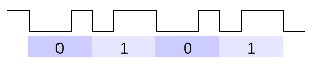 Here the cycles has been evened out to be the same length. The short cycle has been made longer and the longer cycle has been made shorter. The relationship between the high part and the low part of the cycle determines if represents "1" or "0". This makes the bit rate constant regardless of the content.
3. Combination of 1 and 2
Here the cycles has been evened out to be the same length. The short cycle has been made longer and the longer cycle has been made shorter. The relationship between the high part and the low part of the cycle determines if represents "1" or "0". This makes the bit rate constant regardless of the content.
3. Combination of 1 and 2
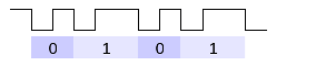 In this case only the length of one half of the cycle determines the bit content. The average bit rate should be the highest of the three but still vary with the content, albeit to a lesser extent.
With some clever coding I hope to support all three variants in the same loading routine.
In this case only the length of one half of the cycle determines the bit content. The average bit rate should be the highest of the three but still vary with the content, albeit to a lesser extent.
With some clever coding I hope to support all three variants in the same loading routine.