There are a lot of fine ham radio transceiver kits and design ideas available today. But the feeling of making long distance contacts using equipment that you have built and designed by yourself excites me. This is what this project is all about. Building a reasonable well performing transceiver while still keeping it simple, modular and, above all, understandable. To begin with I have settled for an SSB only design. While sticking to the modular concept, the plan is to later add more options. I want to get the basic functionally sorted out first.
Below is the initial design I'm aiming at. It's a pretty straightforward single-conversion superheterodyne design.
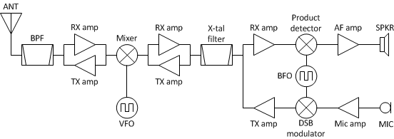
As you can see there are no special features here. No AGC for example at this early experimental stage.
Mixer
I have previously built receivers using the NE612 and while it is a good and versatile mixer it overloads easily. For this design I wanted a signal chain with high dynamic range. Therefore I have settled for a double balanced mixer in the first mixing stage. The DBM is a passive device that has very good mixing performance and does not induce any extra noise.
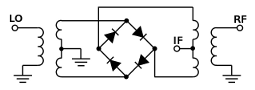
One really neat feature of the DBM is that it is bi-directional which will greatly simplify TX/RX switching. A DBM can be built using two transformers and four matched silicon diodes. They are also available as prefabricated and tested modules from companies such as
Mini Circuits. The
SBL-1 is a high performing and well known DBM. They are definitely more expensive than putting together your own but the performance is solid and they are well encapsulated and isolated. I had a few Japanese SBL-1 lookalikes salvaged from old radio surplus. They would do fine for this build.
Amplifier stages
Several amplifiers are usually needed along the signal path. In my design I've tried to make things simple by using the same amplifier circuit in all low power RF amplification stages. I also wanted a construction based on a common transistor. I picked the BC547B since it's very common, cheap and has reasonable high gain. Other transistors such as BC337, 2N2222 or 2N3904 should work fine too with minor adjustments. The amplifier design has an input and output impedance of 50 ohm and is usable up to at least 50 MHz. Gain is around 12 dB. Many radio designs use a supply voltage of 8V but I settled for the more commonly available 5V supply.
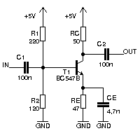
Supply voltage (
Vcc) is 5V. In/out impedance (
Zin &
Zout) is 50 ohm. I set Rc = Zout = 50 ohm.
To determine the collector current
Ic, I set the voltage over
Re to 1.5V. That gives an output swing of 5V-1.5V=3.5V which should be more than enough.
Ic = Vrc/Rc = ((Vcc-Vre)/2)/Rc = ((5V - 1,5V)/2)/50ohm = 35mA
By knowing the voltage over
Re (1.5V) and
Ic (35mA) the value for
Re can be determined.
Re = Vre/Ic = 1.5V/35mA = 47 ohm
Base voltage is determined by the voltage over
Re and the voltage drop over the diode inside the transistor.
Vb = Vbe + Vre = 0.7V + 1.5V = 2.2V
This means R1/R2 should make up a voltage divider that placed the transistor base at around 2.2 volt. The tricky thing with this divider is that is also effects the input impedance (
Zin)!
The complete formula for the input impedance
Zin = R1 || R2 || (Hfe*(re+Re))
Where
Re is the emitter resistor and
re is the emitter resistance inside the transistor.
Re can be omitted by using an emitter bypass capacitor
Ce.
re = 25mV/Ic = 25mV / 35mA = 0.7 ohm
Where 25mV is the voltage drop across the depletion layer of the forward biased diode inside the transistor.
Hfe can be found in the
datasheet of the transistor.
For Ic = 35mA --> Hfe = 200
Complete formula for Zin becomes
Zin = R1 || R2 || (Hfe*re) and after some experimenting
R1 and
R2 can be determined to fulfill both the voltage divider ratio and impedance. I settled for R1 = 220 ohm and R2 = 120 ohm.
Zin = R1 || R2 || (Hfe*re) = 1/(1/220+1/120+1/(200*0.7)) = 50 ohm
By selecting a good value for
Ce the amplifier can be built to reject DC and low frequencies. The -3dB point can be found when the impedance of
Ce is around the same value as
Re.
Zce = 1/(2*PI*f*Ce) -->
Ce = 1/(2*PI*f*Zce)
Setting f = 1MHz and Zce = 47 ohm gives Ce = 3.3nF. I had no 3.3nF at hand so I selected Ce = 4.7nF. Values for C1 and C2 can be reduced for even better rejection of low frequencies if needed but 100nF works fine for basic DC isolation.
My tests shows that the amplifier works surprisingly well for being so simple. It's definitely not the most power effective design but I figure it's and okay trade-of between simplicity and function. In my transceiver this amplifier is used both as RF preamplifier and IF amplifier.
Crystal filter
This is a critical component that greatly affects the performance and selectivity of the transceiver. Usually you would like to have a set of filters to choose from depending on the selectivity and bandwidth required for a given moment. There are many theories behind crystal filter design and in my transceiver I wanted the ability to test various designs. Different filters will most likely have different input and output impedances. Therefore I decided to keep the input and output interface for the filters at 50 ohm. It is easy to adapt filters to 50 ohm using transformers or matching network.
A crystal filter can be assembled using ordinary crystals. A common design is the Cohn filter seen below.
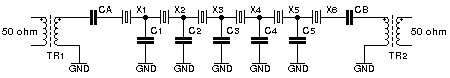
A simple Cohn filter can be constructed using an arbitrary number of crystals and the same value for all capacitors. The naive approach is that the number of crystals determine the filter sharpness and the capacitor values affects the filter width. In reality it's way more complex than that.
In my experiment I tried to create an SSB filter for 8MHz IF. I built a quick crystal oscillator and selected six crystals from a batch of 100 that oscillated within 10Hz of each other. Then I assembled the filter according to the schematic above. Capacitor values of 47pF resulted in a too narrow filter and 22pF was slightly too wide. Clearly this would require some time and effort to get it right. I suspect 33pF will be just about right. Varying the capacitor values greatly affects the filter impedance and it is tedious to rewind the matching transformers every time. One really nice thing I noticed is that an impedance mis-match mostly affects the filter ringing/shape. Therefore it is possible to experiment with different capacitor values first to get the correct width and then afterwards adjust the impedance matching transformers for the best possible filter shape. I used the
miniVNA Tiny for measuring the filter. It really is an invaluable tool for this purpose.
Product detector
In order to receive SSB signals I would need a product detector. The product detector is really just another mixer with two RF inputs and one AF output. For this module I tried another form of mixer based on a HCT4053 switch.
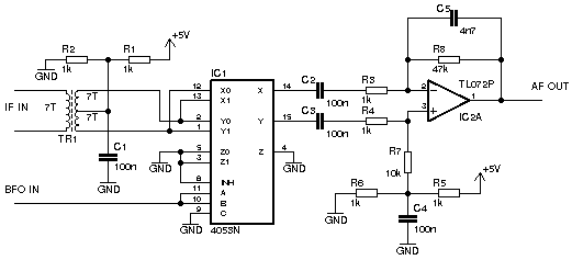
The principle is the same as for the DMB but instead of a diode bridge reversing the current flow it uses a set of CMOS switches that basically reverses the IN/OUT connections at the speed of the BFO. Just as with the DBM, the dynamic range is very high for this construction (limited by the supply rails of the 4053). It is also important to bias the IN/OUT pins to make sure to stay within these limits. I accomplished this by using a resistor divider (R1,R2) that placed the DC level of the input transformer at half the Vcc voltage. At the output of the mixer I did not bother with a transformer. In contrast to the DBM the 4053 does not need to be perfectly terminated for proper mixing. It is however important to make sure the square wave BFO has a 50% duty cycle. The output from the 4053 can be treated as a balanced audio signal that is being amplified and low pass filtered in the TL072 op-amp. The performance of this product detector is surprisingly good despite the simple design. Care must be taken to make sure the op-amp act as a AF low pass filter in order to keep inaudible RF from overloading the AF signal path.
Frequency generators
This construction needs two frequency generators for generating the VFO and BFO signals. In my prototype I have used the
Si5351 chip which is a small and self-contained frequency generator. It has two built in PLLs and three square wave outputs and is fully I2C controlled. Upper frequency limit is about 160MHz. More than enough for a short wave construction. The Si5351 is a very small 3.3V SMD chip but Adafruit makes a good breakout board that is 5V tolerant and also contains a built in 25MHz reference oscillator. For the prototype I put together a temporary box containing the Si5351 generator module from Adafruit, Atmega328 micro controller, HD44780 LCD, rotary encoder and a few buttons. More information on this will follow.
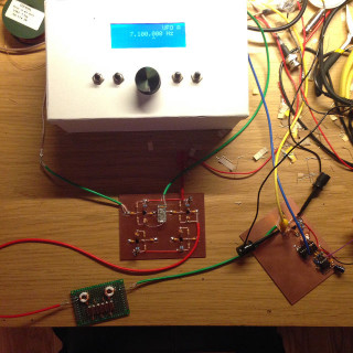
Working prototype
Stay tuned for the next part of this project writeup!