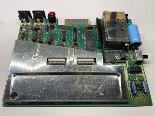
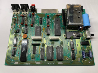
Back in the day Hewlet Packard used to make really nice test instruments. That division later became Agilent, which still makes nice instruments, but there is something special about the vintage HP stuff. The substantial part of my lab consists of vintage HP gear. I really like the look and feel of them, and they are maintainable in a way that, in my opinion, current instruments generally never will be. They also come with beautiful manuals that not only tell you how to operate the instruments but also, in great detail, how they work. Even now, several decades after production it's still possible to source or manufacture parts to maintain these instruments. In some cases HP made their own special original parts that makes service a bit difficult. One such situation is the RF power meter sensor heads.

The HP RF power meters were very good performers when they came out. They consisted of the meter itself that resembled the usual HP series of instruments, but they also relied on interchangeable sensor heads. That made it possible to use the same meter with different sensor heads with different specifications and for different purposes. All well and good. The big problem here is that the sensor heads are easy to damage by running them out of specifications (like over power or input DC). What makes this even worse is that all of the HP sensor heads are made with HP special parts that are nowadays unobtainium. This has led to an abundance of cheap HP RF power meters on the market but very few matching sensor heads, and without a sensor head the meter is unusable.
I have attempted to re-create a sensor head that can be used with the HP 435A, 436A and 438A series meters.
RF power sensor types
Most of the RF sensor heads HP made for these meters were thermocouple based. Simply put, they work by dissipating the incoming RF energy into a load resistor and then measure the increase in temperature of that resistor using a thermocouple and something like a Weatstone bridge to determine the RF power. They can be made to have great performance and accuracy but are generally not well suited to measure very low power levels. They are also difficult to DIY.
Another very common way of measuring RF power is a diode based sensor. It also works by dissipating the RF energy into a load resistor but instead of measuring temperature it measures the voltage across the resistor. This will be an AC voltage that can be rectified into DC using a fast diode. The diode sensor is not as accurate as the thermocouple sensor but can measure very low levels. The main drawback is that it is greatly affected by the linearity and temperature coefficient of the diode. HP made one popular RF sensor head of this type called the 8484A.
My first attempt will be to see if I can build a diode based RF sensor head, similar to the 8484A, that can be interfaced to an HP 435A, 436A or 438A power meter.
HP sensor theory of operation
All HP power sensors of this type consists of what HP refers to as an
RF bulkhead assembly containing the input RF connector and either the thermocouple or the diode based detector. This is a very special and custom HP part that is not easily reproduced. The reset of the sensor is a fine tuned chopper-amplifier. Or rather one half of a chopper amplifier. The other half is in the meter itself.
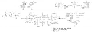
Below is the schematic for the HP 8484A diode based power sensor head. The schematic does not reveal details around the HP RF wizardry but it does show the basic electrical construction. Major parts of what makes the HP sensors perform well is in the mechanical construction and component selection, many of which are HP custom. Completely replicating this today is more or less impossible but we can make reasonable assumptions and perform component substitutions to get us well on the way.

A1 in the schematic is the venerable bulkhead assembly. In this case a diode detector encased in a carefully crafted aluminium shell to optimize frequency response and SWR, all interconnected using spot welded gold wires to minimize thermoelectric effects. Here is where my design have a very tough time trying to keep up with the original.
A2 is the chopper-assembly. This is the PCB in the sensor containing the first part of the hi-gain chopper amplifier. Even though it's a relatively regular thru-hole design the two chopper FETs are on a special shared HP silicon substrate. The two output gold wires from the bulkhead assembly are press-fit onto this substrate, again to minimize thermoelectric effects. The rest of the circuit is a relatively simple amplifier stage. The biggest problem here is to find suitable transistors to use for both the FET-chopper switches and the amplifier. This resulted in a lot of trial and error. Not only is the component selection critical, but the actual layout and signal routing plays a very big part in this.
The chopper frequency is around 200Hz and is supplied by the meter as two 180 degrees out of phase signals. One for each chopper FET. The timing of these signals is very critical. More on this later.
In order to support multiple sensor heads of various ranges the meter display can show different ranges. The range however is not user selectable but instead a resistor in the sensor head tells the meter which display range to use. HP calls this the
mount resistor and has to be one of a few discreet predefined values corresponding to the available ranges. The resistor forms one part of a voltage divider that drives a set of comparators in the meter.
The sensor head connector
In order to even get started I needed a way to connect things to the meter's sensor head input. The connector here is a bit unusual but not HP proprietary. It's an C091 series connector from Amphenol. The connector I found that matched the HP original is the 12pin
T3638-004 connector. Even though they are relatively expensive at 30 euro a piece, they are still available.
Detecting RF power
The second core part needed was a reasonably well performing diode RF power detector. After some digging I decided to try basing the detector around a BAT62 diode. More precisely the BAT62-02V from Infineon. It's an RF diode that I assumed would be well suited for situations like this. In the end I did not try any other diodes since this one worked quite well.

The detector can be seen above. Physical design is important here in order to achieve good performance. I decided to build the detector directly onto an PCB SMA connector using SMD components. The 50 Ohm load is made up using two 100 Ohm 0805 resistors in parallel soldered directly onto the base of the SMA connector to dissipate heat into the housing. The diode is then soldered onto the tip of the center pin, away from the load resistor heat source, and held in place using the two filtering capacitors. This design needs more work but it performed reasonably well up to a few GHz and was good enough for me to continue working on the chopper amplifier part of the sensor.


The first experiments with the chopper design was made using flying point-to-point assembly to reduce lead lengths and influence by board substrate. It quickly became apparent that the HP design was very sensitive to the physical layout. At first I tried to reproduce the circuit using modern transistors but it was difficult to make it stable. Without knowing the exact specifications of the original proprietary HP transistors I had to guess here. In the end I opted for older/slower transistors that was less temperamental and performed much better and probably also more closely matched the originals in the HP design.
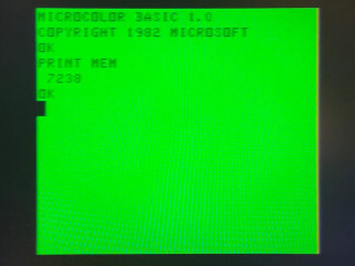
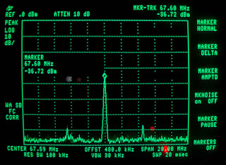
Using a precision DC source as a substitute for the diode detector I was able to get the HP 436A to display any value within the selected range and hooking the diode detector up to the chopper amplifier did indeed produce reasonable results. To generate the very small DC levels needed I actually did not use a DC source per se, but an HP 6181C current source and a very small shunt. It's an easy trick to generate low-noise DC.
Below is a few images of the first substrate-less prototype on the bench. It could detect signal levels from around 0dBm down to -30dBm but below that it was too noisy. It really needed to be shielded. After shielding it reached down to -40dBm and the entire range was a lot more stable. The thermal mass of the enclosure also helped stabilize the readings. No wonder the HP 8484A sensor is encased in a big chunk of machined aluminium.


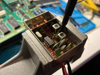
I found a nice aluminum enclosure that could fit an N-connector directly at one end but the C091 connector at the other end was a tight fit. I ended up using my CNC mill to get the mounting hole placed exactly where I wanted it. Drilling a big hole in a small piece of thin sheet metal can be tricky. Now on to cleaning up the inside.
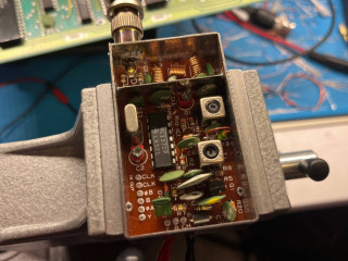
My first proper version of the sensor
Below is a schematic of the latest iteration and it took quite a while to get here. Keep in mind that the schematic alone is not enough to build a working sensor. The assembly itself is very critical.

For the chopper transistors, Q1 and Q2, I used a pair of BF256B FETs that has to be reasonably well matched (it may take a few tries), and in order to improve temperature stability I also glued them together. This is probably the most sensitive part of the circuit. Putting Q1 and Q2 onto a PCB is difficult. The inputs to Q1 ad Q2 should not be routed on a PCB and must consist of as few materials as possible to avoid thermoelectrical affects (resistors R1 and R3 helps limit this to some extent). In my design the output of the diode detector is directly soldered onto the inputs legs of the chopper FETs.
The 200Hz chopper gate drive signals that controls these switches is very sensitive. The input capacitance of the FETs affect the switch timing and has to be adjusted very carefully. In the schematic there are two capacitors, C2 and C3, between gate and ground on each FET. In reality only one of them need to be fitted. The capacitor(s) need to be selected experimentally for best zero reading on the meter. In the original design HP used two flying wires for these signals that went directly from the connector to the FET inputs. The timing could then be even more fine tuned by wiggling the two cables around for the best reading. I found that I could route both signals together in a screened cable from the connector all the way to the FETs with good results with the screen connected on one end to the guard ground, and then carefully select capacitors C2 and C3.
The amplifier transistor Q3 is less critical. Here I found that a BC337 of similar age and generation worked well. The gain of the amplifier can be tweaked by varying R7. Here the gain has to be selected to match the measurement range of the sensor. In my case I selected a mount resistor value of 22k which set the range to -40dBm to 0dBm to match my diode detector.


Conclusion
It is really difficult to construct a high performing RF sensor. I understand that now more than ever. The fact that HP managed produce these high performing sensors in great numbers with strict specifications is impressive. No wonder they were expensive and still is. I'm very pleased that I managed to cobble together something similar and compatible that is actually usable, and made using only current off-the-shelve parts.
My sensor head is definitely not in the same class as the originals, but for most stuff that I do it's enough. And more importantly, I can use this cheap and easily reparable sensor head to verify unknown signals before risking any of the fine HP sensors and their unobtainium parts.

Image above showing my sensor to the right together with two common HP sensor heads. The 8484A diode based sensor and the 8482A thermocouple based sensor.
This new sensor has quickly become my go-to sensor in the lab. I really like that it is small and light. That means less risk of breaking whatever it's hooked up to. I'm tempted to make an SMA version. That N-connector is good and robust but many modern devices use smaller connectors. The lightness has it's downsides too. The original sensors are heavy because they are very well shielded and has a bigger thermal mass. My small sensor has more input filtering to mitigate the extra noise, but that also makes it slower. It is also more susceptive to sudden temperature changes. Like hand holding, which is always sensitive with these sensors but it becomes more apparent with a small thermal mass.
Next step
I'm curios to explore other diode detector constructions. The detector I put together here can be made to perform better in may ways. With other detectors other ranges would also be possible. I find the -40dBm to 0dBm range to be quite useful for what I do, but sometimes a little more sensitivity would be useful. The linearity of most diodes are better a lower levels. Maybe even combine a diode detector with a built in fixed attenuator would be an option. That could also improve SWR. There are also many new integrated RF detectors. Maybe some of them could be used as a front end detector. They do however need a DC supply which does not exist in the cable. Maybe the relatively powerful chopper signals can be used to extract power. Many options to consider. To be continued...