2013-12-11 07:52 UTC
In order to try out the new I/O expansion bus for the MC3 I built a few quick I/O boards. The first one is a simple 8-bit DAC. I had an
TLC7524 laying around. It's a simple DAC to interface to my bus since it has a built in latch. The analog side of this chip is however a bit confusing. After digging through the datasheet for quite some time and not really liking the example circuits I eventually focused my attention on the figure on page 5 - "voltage mode operation".
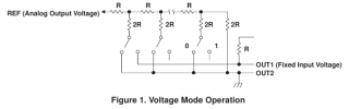
This figure from the datasheet shows the resistor ladder at top and the digital switches beneath. In the application examples the REF pin is an input and the OUT1 and OUT2 are outputs feeding a differential amplifier but from this vague description I figured it might be possible to make it work the other way around with the REF pin acting as a single output. In that case OUT1 and OUT2 would be connected to Vcc and GND respectively to set the upper and lower limit of the DAC output. A much more simple design.
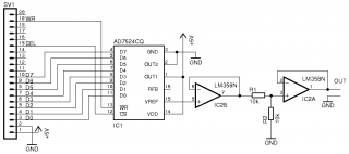
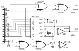
Below is the schematic of my DAC board. The symbol is actually an AD7524 since it was the only one I had in the symbol library but the pin-out is the same as for the TLC7524. I added a voltage following op-amp as a buffer for the output and divided the output from the DAC.
IMPORTANT: Check out Kevins version and comments below before building this yourself
MK1 version - good for audio
 Update 2014-01-26
With the above circuit one could guess the output swing would be 0-2.5V with the 1:2 voltage divider but the divider and op-amp puts too much load on the DAC output and lowers the final output. Thank you Leo Bolier for pointing out this issue. The MK2 version buffers the output before the divider and improves the situation.
MK2 version - higher output
 Update 2014-03-23
I ended up going with the MK1 version. It's just right for my needs.
This is what the MK1 output looks like on a scope running a simple loop to generate a sawtooth.
LOOP	INCA
	STAA	DAC
	BRA	LOOP
Note: Using the operation 'INC DAC' will not work here since the DAC value is not readable.
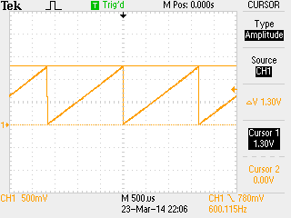
As you can see the output voltage at $FF is only 1.3V. For my case this is perfectly adequate and the linearity is good.
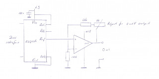
Update 2014-03-25 - Leo Bolier's version
Leo kindly sent be his DAC design. This one is more elegant with an adjustable output and higher range.
Thank you for sharing!
This is how my (MK1) board ended up
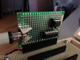
An RCA jack for output.
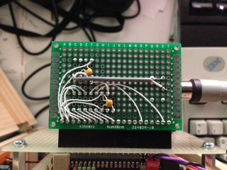
A quite tidy backside. I was lucky that the arrangement of the DAC data pins matched my bus connector.
The DAC boards occupies the whole 16 bytes address space of the I/O slot it uses but since I'm unlikely to place any other chips on this board I don't expect this to be an issue.
Despite not taking any special actions to filter the supply or signal paths the noise level on the output is actually fairly low when used as an audio device connected to a line input. This could definitely be improved but I do not feel the need for it.
Update 2014-06-23
A DAC can be quite useful as a debugging tool when connected to a scope. Writing debug values to the DAC and being able check for timing is one really nice feature to have. The problem can sometimes be to know when to actually trigger the scope for a stable display. Therefore I have added a separate TRIG output to my DAC board. The TRIG output generates a pulse when the DAC is being written to when A0=1 and omitted when A0=1. That way it is possible to select when a TRIG pulse is generated.
MK3 version - trigger output
Below is an example when the scope triggers on the TRIG signal and after that a series of 14 values are written to the DAC.
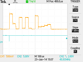
Channel one is the DAC output and channel two is the TRIG output.
Update 2015-10-02 - Kevin Baker's version
Kevin kindly shared an elegant way of doing this. See his comments below. Thank you Kevin!
by Leo Bolier 2014-01-23 14:25 UTC
I build this circuit but had to use an AD7524 since that was the only laying around. However it did not work as described above. The power supply (and thus the voltage on OUT1 ) was 5 V. With all '1' on the data latches the output voltage on Vref was a little less then 2.5 Volt. Increasing the voltage on the OUT1 pin to 12V (leaving the supply a 5V) did not work. The maximum output voltage stayed at this 2.5Volt. When I also increased the supplyvoltage till 12V the whole DA conversion ceased to work. When you look at the datasheet of the AD7524 the chapter of voltage mode is missing. It seems there is a design difference in both devices. Anyone has a clue ?
by Daniel 2014-01-24 08:43 UTC
Interesting discovery Leo. I have always assumed the AD7524 and the TLC7524 to be interchangeable but from your tests it looks like that is not the case. I had a look in the AD7524 datasheet and indeed there is no mention of a voltage mode as in the TI datasheet. I wonder what may be the difference. At least the functional block diagrams of both devices look very much the same.
by Leo Bolier 2014-01-24 09:25 UTC
First I thought the msb of the latch was gone but that proved not to be the case. Then I mistrusted the opamp. But even without the Opamp circuitry, so a bare 7524 the result remained the same.
I repeated the test with 2 other AD7524 devices (just to be sure). Results are almost the same. The 2.5 max output voltage was a little less. Because I need 5 volt output I bypassed the problem by replacing the voltage follower with a non-inverting x2 opamp but I remain curious. Another point of interest is that the AD7524 schematic calls the values of the resistor network 10K and 20K. The TSC spec does not say so. Last but not least both specs call the resistance between Vref (15) to ground to be 5k to 20K. I presume with all switches closed till all switches open. When looking at the schematic I makes you wonder. With all switches open the resitor network seems to be floating with respect to Gnd.
by Daniel 2014-01-26 19:23 UTC
Perhaps there is something going on with the switches within the DAC that we don't know. I believe the datasheet(s) doesn't really tell what kind of switching technique that is actually used. I'll make some quick tests.
by Daniel 2014-01-26 21:16 UTC
You are right! I did some more testing and got interesting results. I was too focused on the linearity of the signal and did not notice that the final signal level was actually lower than expected.
I believe that the formula in the TLC7524 datasheet is theoretically correct.
Vo = Vi*(D/256) -> [D=256] -> Vo = Vi
However, since R may be in the vicinity of 10k or more, the output impedance of the DAC is fairly high. Thus my external resistor divider lowers the signal more than I expected. I disconnected the divider and put a high impedance meter directly on the output pin. The level was then about right but as soon as I began loading the output the level also dropped significantly. The linearity of the signal was however still good.
by Leo 2014-02-14 15:49 UTC
Daniel,
Haven been away on vacation to Madeira for a week so my reaction is a little late. I think the Tlc and AD7524 have basically the same design. For some reason the manufacturer of the AD does not mention this voltage mode operation. For me case closed.
by Daniel 2014-02-19 06:15 UTC
I agree Leo. Case closed. Hope you had a joyful vacation. Thank you for reading!
by Leo 2014-03-15 22:00 UTC
Daniel,
Forgot to mention: you can save half an opamp by using a non-inverting opamp that gives a high input impedance and (if required) an adjustable gain. Because I need a 0-5V output the opamp has +12V as powersupply. I can send you a schematic drawing if you want.
by Daniel 2014-03-23 21:44 UTC
Hi Leo!
Thank you for the input. You are absolutely right. Using an op-amp with some gain would be the proper way to do this. I updated the page here now showing that I ended up leaving my design as is was in the first place anyway. As it comes around it's well suited for line level audio and that's what I ended using it for. Please share your design if you want. I can place it here on this page with credits to you. Thanks again!
by Leo Bolier 2014-03-25 08:56 UTC
Daniel,
I tried to mail a scan of my design to contact(at) waveguide.se but the email got returned. See errormessage below;
contact@waveguide.se
SMTP error from remote mail server after end of data:
host mail.waveguide.se [89.253.123.242]: 550 IP listed in recent.spam.dnsbl.sorbs.net
by Daniel 2014-03-25 09:16 UTC
Leo, I salvaged your mail from the filter. Thank you! Check your inbox ;)
by Mats 2015-04-21 07:43 UTC
Hej Daniel!
I´m using the tlc7524 to control a VCA in a filter circuit. But im having problem with voltage loss in the DAC. Did you experience this? If i put 5V in on all pins i get 4.2V out(supply voltage is 5.2V). I have tried putting a voltage follower after the DAC and a 1M resistor to get the voltage out but nothing helps.. seems the datasheet formula (Vo = Vi) is lying =)
by Daniel 2015-06-29 11:22 UTC
Hej Mats! Your results are indeed consistent to mine. I suspect the formula in the datasheet is simplified in some way and not telling the entire truth. The design proposed by Leo presented above may be the best solution if full swing is really needed on the output. Good luck with your project! :)
by Kevin 2015-10-02 16:59 UTC
In trying to use multiple sources for this DAC, I came across the differences in trying to use them in "voltage mode". I evaluated the TI TLC7524, Maxim MX7524 and Analog Devices AD7524. They all function in this mode, but differently. If you notice on the TI datasheet where it discusses operating in this mode, the spec for the reference voltage is only 2.5V when the device is operating at 5V, and this is the key to the differences.
With a Vref of 5V, the TI part had a swing of about 4.2V, the AD part had a swing of about 2.5V and the Maxim part had a swing of about 3.1V. The waveform generated was a sawtooth, and all devices showed nonlinearity at the high and low extremes.
With a Vref=2.5V, all parts had a swing of about 2.5V, with slight nonlinearity at the low end.
I was able to find some notes on the voltage mode in regards to the AD device, with the caveat that the reference should be between 0.8 and 1.3V for best linearity.
I am using these devices with a 1.25V reference and expect good results using devices from any of those manufacturers.
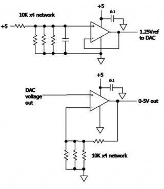
If one is not looking for absolute accuracy, one solution is to use a couple of resistor networks for best matching and temperature tracking. I chose networks with four 10K resistors. I use one network to derive 1.25V from the 5V supply and buffer that with a unity-gain op amp before going into the reference input (Out1). I use the second network around an op amp on the DAC output (Ref) to provide a gain of 4. Assuming rail-to-rail op amps, this gives a full-scale 5V output, and it tracks the reference voltage perfectly.
by Daniel 2015-10-02 19:02 UTC
Nice! You're the man Kevin! Your work is highly appreciated. Thank you for sharing.
Do you mean that simply lowering OUT1 voltage to Vcc/2 would improve the linearity but still maintain a lot of the output swing?
by Kevin 2015-10-02 19:30 UTC
Lowering the reference voltage (OUT1) helps to allow devices from different manufacturers to function alike. They all still have a bit of non-linear "tail" on the low end with a 2.5V reference. Based upon the comment about the Analog Devices device, I would not run the reference over 1.25V.
My design uses a divide-by-four for the reference voltage, and a multiply-by-four gain stage for a swing of Vcc. The voltage divider and gain stage complement each other and will help ensure a full swing of Vcc, even if Vcc changes. If one were to use a fixed reference and then a gain stage, the output may not swing all the way to Vcc, or if Vcc were low, the op amp might saturate at a digital code of well below 255.
This is a good way to do a ratiometric converter, where absolute voltage accuracy is non-critical. For absolute accuracy, the circuit would need a few slight changes, which could be as simple as a very accurate 5V supply and high-precision resistors.
Make sure to use a good-quality, rail-to-rail op amp, such as the LM6134/LM6144, or the MCP6294. Those amps get within millivolts of either rail.
by Leo 2015-11-11 10:29 UTC
Hi again Daniel,
Interesting news about using a ref voltage of 1.3 max.
My focus was on output swing and not so much on linearity.
My project for this d/a converter design was stuck for a while. I intent to continue in the next months.
by Antonio 2022-04-10 19:42 UTC
We are now on year 2022. Perhaps is too late to put here a comment, but I agree that the data sheet of TLC7524 is very confusing. The description is nothing but unclear. I always remember the books of National Semiconductors with well planned descriptions and lots of applications.
Write a comment