I'm happy to admit that while progress has been slow, the transceiver project is not forgotten. As always, many things are competing for their share of my spare time. It will be finished. Eventually.
In
part one I presented the basic concept, first prototype and the main analog parts for the receiver (some of which will be used for transmit as well). While I have the basic analog concept working, my transceiver will not be of much use in the shack without a pretty box and a good way of controlling it. This part of the build is about the microcontroller, LCD and buttons.
The first thing I did was to locate a suitable enclosure. The loose-boards-all-over-the-desk-design was getting difficult to manage even for a prototype build. Ideally a metal enclosure would be better but I went for plastic simply because it's easier to work with and I'm counting on not getting everything right the first time anyway.
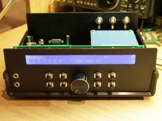
One basic requirement I had with this design was that I wanted the ability to control all of the transceiver functions remotely from an external computer. That includes various analog gains and volumes. It would need some extra work but in the end I think it will be worth it. The first prototype used a 4x20 character LCD but I've now changed it to 2x40 character LCD to make better use of front panel surface area. To keep it simple I also wanted to base the logic around the
Atmega 328 since it's a very common microcontroller today. It may be a bit under powered for what I want to do but with some efficient code I think I can pull it off. I'm not a huge fan of the Arduino so software will be written in
C directly for the Atmega using
avr-gcc that hopefully also saves me some program space. Not entirely knowing yet how I want the user interface to work I just mounted a set of eight buttons. There is still room for more if there is a need for it. All buttons are momentary. Also on the front are two stereo jacks for headphones and microphone with PTT button.
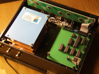
The inside is divided into two stacks of half size euroboards. The left stack above contains three boards for the RF parts (top board currently empty) and the right side will be a stack of two boards for the digital and audio parts (only the digital board is in the picture). In the space between the stacks I will squeeze in a vertical board for the crystal filters (not sure how many I will be able to fit in there but hopefully at least two). On the rear panel I have mounted three BNC connectors. Not yet sure how they will be used but hopefully switchable antennas and IF in/out. Also on the back is a DB9 for RS-232 that will be connected to the Atmega 328 UART for remote control. Of course there is also a DC-jack.
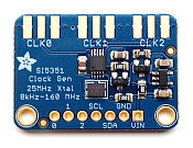
As mentioned in part one of the project I have chosen the
Si5351 frequency generator for VFO and BFO. Controlled by I²C it's a good match for the Atmega 328. Adafruit has a nice little board for this chip that contains a pretty decent reference oscillator, I²C level converters and it's own 3.3V regulator. The Si5351 has three outputs but there are actually only two PLLs inside meaning that I can only get two totally independent frequencies out of this chip but it will be enough. My plan is also to glue a suitable I²C thermometer to the board and isolate it in it's own little enclosure. That way I can compensate for temperature related frequency variations in software.
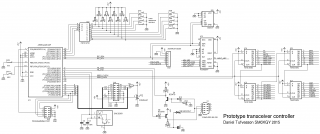
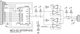
Above is my current draft schematic for the digital controller board. I tried to make decent use of the Atmega 328 I/O pins. Front panel buttons are connected to a '174 encoder that gives me a total of nine buttons on only four I/O pins. Pretty efficient with the downside that only one button can be pressed at a single time. User interface will have to be designed around this limitation but I don't think it's a big issue. The encoder knob is connected to the INT0/INT1 pins that have flexible interrupts. Decoding in software really needs to be interrupt driven not to mis a step. On the I²C bus I have the Si5351 board, a DAC/ADC (PCF8591) and an EEPROM. My plan is to use the DAC/ADC for reading incoming signal level, RF power etc and for software based AGC. Still need to work out how to do this in detail. EEPROM will be used for settings and calibration data. Another suitable multichannel volume control chip will also be connected to the I²C bus for the audio routing and levels. The four '164 shift registers provides a total of 32 outputs for controlling various functions. The PTT and CW key have their own pins so that they are not interfered by other key presses.
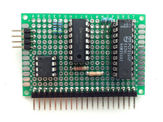
I have written rudimentary code to test and verify all parts but it's not release-ready. From the image above you can get the basic idea of what the interface looks like right now.
That's about it for now! Hopefully the next update will not be that very far away this time.
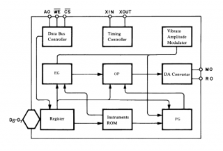 This is the bock diagram of the YM2413. It has a simple 8 bit bus interface with one address line. A quite common interface for this kind of device. This way the chip has two registers. One for selecting among the 271 internal register bits of audio generating goodies and one for writing data to them. There is no way to read back anything usual from the YM2413 so I consider it as a write only device. On the analog side there are two outputs. One for melody and one for percussion. I suspect the reason for this is to keep them on separate audio paths for filtering and mixing but really all designs I have seen treats them equally and mixes them together.
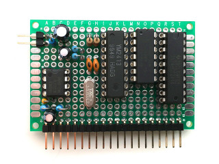
Below is the board I ended up with. It could have been made using fewer chips but as with the YMZ284 board I wanted to isolate the YM2413 from the bus as much as possible.
This is the bock diagram of the YM2413. It has a simple 8 bit bus interface with one address line. A quite common interface for this kind of device. This way the chip has two registers. One for selecting among the 271 internal register bits of audio generating goodies and one for writing data to them. There is no way to read back anything usual from the YM2413 so I consider it as a write only device. On the analog side there are two outputs. One for melody and one for percussion. I suspect the reason for this is to keep them on separate audio paths for filtering and mixing but really all designs I have seen treats them equally and mixes them together.
Below is the board I ended up with. It could have been made using fewer chips but as with the YMZ284 board I wanted to isolate the YM2413 from the bus as much as possible.
 Have a look at the schematics below. U1 and U2 could have been excluded for simplicity but they do wonders for suppressing audible noise from the bus. They also protects the YM2413 from the outside world.
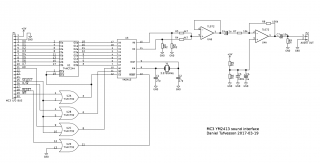 On the analog side of the YM2413 I have mixed together the MO (melody output) and RO (rhythm output) signals as suggested in the application manual. They are then fed into a high impedance voltage following TL072 op-amp to maintain as much of the signal integrity as possible. Some designs suggest adding a capacitor to make up a passive low-pass filter to get rid of high frequency sampling products but I did not want to put additional strain on the outputs. This kind of filtering can be done at a later stage if needed.
Following the high impedance buffering stage I had to add an amplification stage since the signal levels coming from the YM2413 is actually pretty low. This stage is made up using the second part of the TL072 working as an AC-coupled inverting amplifier centered around Vcc/2. I had to make the amplification a factor of 10 to achieve decent line levels on the output. I was a little surprised about this but looking at other designs this seems to be normal. The output of the YM2413 is a lot lower than the YMZ284. Because of all this amplification the YM2413 is noisier than the YMZ284. But then again, It's a totally different chip. One could reason that given the many channels in the YM2413, more headroom is needed and therefore a lower total output per channel.
I mentioned earlier that this was a cost reduced version of the Yamaha OPL. One main reason is that it has 16 selectable instruments out of which only one is customizable. The other 15 are stored in the built-in ROM. This of course reduces the flexibility of the chip but it also makes it easier to get started.
On the analog side of the YM2413 I have mixed together the MO (melody output) and RO (rhythm output) signals as suggested in the application manual. They are then fed into a high impedance voltage following TL072 op-amp to maintain as much of the signal integrity as possible. Some designs suggest adding a capacitor to make up a passive low-pass filter to get rid of high frequency sampling products but I did not want to put additional strain on the outputs. This kind of filtering can be done at a later stage if needed.
Following the high impedance buffering stage I had to add an amplification stage since the signal levels coming from the YM2413 is actually pretty low. This stage is made up using the second part of the TL072 working as an AC-coupled inverting amplifier centered around Vcc/2. I had to make the amplification a factor of 10 to achieve decent line levels on the output. I was a little surprised about this but looking at other designs this seems to be normal. The output of the YM2413 is a lot lower than the YMZ284. Because of all this amplification the YM2413 is noisier than the YMZ284. But then again, It's a totally different chip. One could reason that given the many channels in the YM2413, more headroom is needed and therefore a lower total output per channel.
I mentioned earlier that this was a cost reduced version of the Yamaha OPL. One main reason is that it has 16 selectable instruments out of which only one is customizable. The other 15 are stored in the built-in ROM. This of course reduces the flexibility of the chip but it also makes it easier to get started.
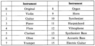 The table of instruments can be seen above. Instrument 0 is the user customizable instrument. The others are preset by Yamaha and it's not really a bad thing. They are well made and well known from other Yamaha keyboards and General MIDI.
Since FM generation is not very good for creating percussion sounds there is a separate percussion module in the YM2413. It consists of the basic kit of base drum, snare drum, tom-tom, top cymbal and high hat.
The table of instruments can be seen above. Instrument 0 is the user customizable instrument. The others are preset by Yamaha and it's not really a bad thing. They are well made and well known from other Yamaha keyboards and General MIDI.
Since FM generation is not very good for creating percussion sounds there is a separate percussion module in the YM2413. It consists of the basic kit of base drum, snare drum, tom-tom, top cymbal and high hat.
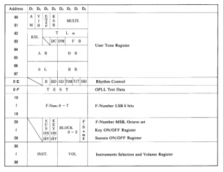 This is the register layout of the YM2413. FM sound generation can get pretty complex but this is about as straight forward as it can be. Please read the datasheet and application manual for more info. I really wish the application manual had more examples. I still have a lot to figure out.
YM2413 datasheet
YM2413 application manual
This is the register layout of the YM2413. FM sound generation can get pretty complex but this is about as straight forward as it can be. Please read the datasheet and application manual for more info. I really wish the application manual had more examples. I still have a lot to figure out.
YM2413 datasheet
YM2413 application manual